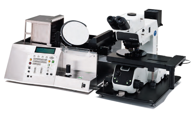
The ability to accommodate different wafer sizes is a key for expanding fabs. The AL120 series consists of three models based on wafer diameter, the 200 mm (AL120-L8), the combination 150 mm and 200 mm (AL120-L86) and the 150 mm model for wafer sizes of 150 mm or less (AL120-L6). Each system is designed for wafer transfer and microscope inspection. Topside and backside macro inspections are also available for all wafer sizes.
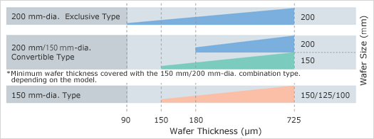
Wafer Size and Thickness
To meet the demands of thin wafer manufacturers, the new arm design of the AL120-LMB-90 model can handle a full cassette of 90 µm wafers.
Inspection parameters and recipes of the AL120 can be controlled through an optional RS232C serial interface. Equipment manufacturers and labs with internal inspection software can enhance automation and efficiency by incorporating the AL120 Wafer Handler. The serial interface uses Dynamic Link Library (DLL), making integration simple with application specific software.
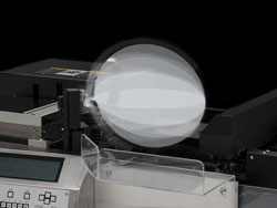 Macro Inspection - 360 Degree Rotation (Simulation)
The AL120 interfaces with the Olympus MX series of dedicated wafer inspection microscopes that provide exceptional image resolution and clarity through a wide range of observation methods including brightfield, darkfield, differential interference contrast (DIC), near-IR (near-infrared) and DUV (deep ultraviolet). The motorized objective turret and aperture stop are interlocked, allowing optimal illumination and contrast of each objective lens. The AL120 can also be adapted to other microscope models on a special order basis.
| Wafer Loader AL120 Specifications*1 | ||||||||
| 200 mm Type | 200 mm / 150 mm Convertible Type | 150 mm Type | ||||||
| AL120- LMB8- 90 |
AL120- LMB86- 180 |
AL120- L86- 180 |
AL120- LMB86 |
AL120- L86 |
AL120- LMB6- 150 |
AL120- L6- 150 |
||
| Wafer Size (SEMI Standard) | 200mm | 200mm / 150mm | 150mm / 125mm / 100mm |
|||||
| Minimum Wafer Thickness | 90µm | 180µm | 400µm | 150µm | ||||
| Type of Cassette*2 | SEMI stad. 25 (26)-slot | |||||||
| Number of Cassette | 1 | |||||||
| Inspection Recipe | All / Sampling | |||||||
| Inspection Sequence | Micro (Microscope) | YES | YES | YES | YES | YES | YES | YES |
| Top Macro | YES | YES | YES | YES | ||||
| Back Macro | YES | YES | YES | YES | ||||
| 2nd. Back Macro | YES | YES | YES | YES | ||||
| Wafer Orientation (Every 90°) | Non-contact (O.F./Notch) | Non-contact (O.F.) | ||||||
| External Control*3 | YES | YES | YES | YES | YES | YES | YES | |
| Compatible Microscope Model | Olympus Semiconductor Inspection Microscope MX61 | |||||||
| Dimensions (mm) | 640 (W) x 620 (D) x 378 (H) Body Only, 1100 (W) x 620 (D) x 378 (H) with Microscope | 570 (W) x 620 (D) x 400 (H) Body Only, 980 (W) x 620 (D) x 400 (H) with Microscope | ||||||
| Weight (kg) (Main Body Only) | 44 | 44 | 41 | 44 | 41 | 40 | 37 | |
| Utility (Power Consumption/Vacuum) | AC100 V - 120 V, 1 A, or AC 220 V - 240 V, 0.5 A 50/60 Hz, -67 to -80 kpa, 20 Liter/min or higher | |||||||
*1 All types of wafers must be tested in advance, please contact your local Olympus office.
*2 Up to 10 types of wafer and/or cassette combinations can be registered at one time.
*3 Optional interface, Compatible OS: Windows7 (32-bit/64-bit)
If you have question you can reach us. Just fill up the form below.